
Non-Contact Sub-Pixel Automated Edge Detection Algorithms in Electronics QA
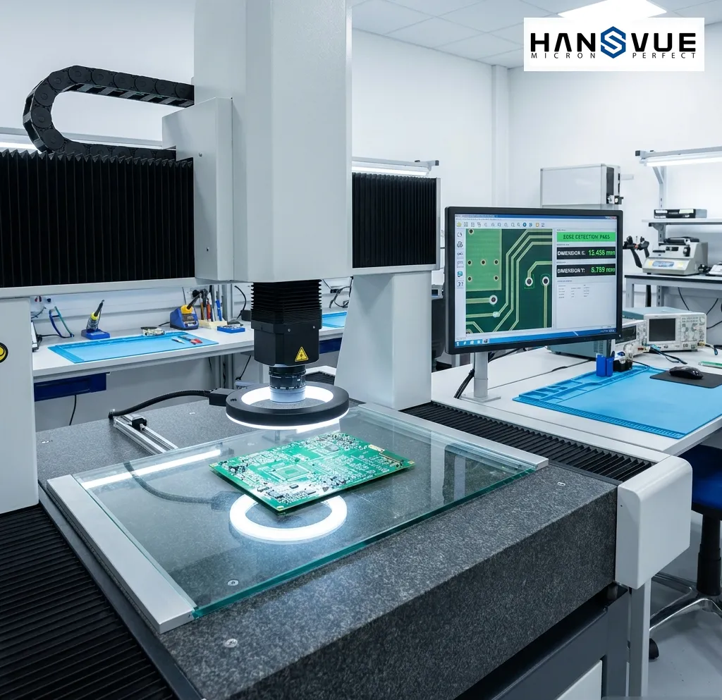
Automated Non-Contact Measurement in Electronics QA High-density electronics manufacturing requires rapid dimensional verification of micro-connectors, SMT componentleads, and flexible printed circuits. Automated Video Measuring Systems (VMS) combine optical cameras, precision motorized stages, and advanced software algorithms to automate batch inspection. How Does Sub-Pixel Edge Detection Achieve High Measurement Repeatability? Sub-Pixel edge detection achieves high measurement […]
Root-Cause Microstructural Failure Analysis of Intermetallic Compound Fatigue and Crack Propagation in Electronic Solder Assemblies
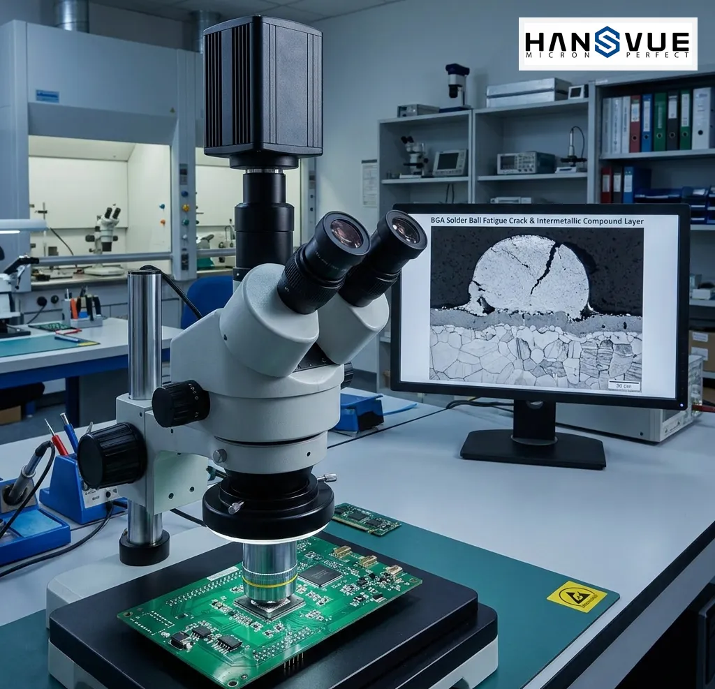
In modern microelectronics manufacturing—spanning automotive Electronic Control Units (ECUs), 5G telecommunications infrastructure, and aerospace avionics—solder joint structural integrity directly dictates field reliability. Transitioning to lead-free solder alloys (SAC305, SAC405) under RoHS environmental mandates has introduced heightened susceptibility to intermetallic compound (IMC) embrittlement, thermal fatigue micro-cracking, and electromigration voiding. Failure of a single BGA solder sphere […]
White Light Interferometry vs. Confocal Microscopy in 3D Optical Surface Profilometry
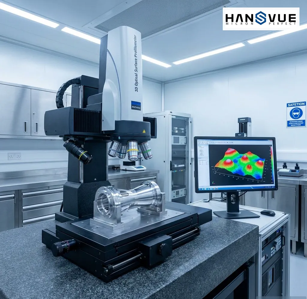
High-Precision Optical Metrology in Modern Manufacturing Surface finish evaluation is critical for high-performance mechanical components, micro-electronics, and polishedoptical molds. Achieving nanometer-level vertical resolution requires non-contact optical profilometry, eliminating thephysical scratch damage caused by traditional diamond-stylus profilers. How Does White Light Interferometry Achieve Sub-Nanometer Resolution? White Light Interferometry achieves sub-nanometer vertical resolution by splitting a broadband […]