
In modern microelectronics manufacturing—spanning automotive Electronic Control Units (ECUs), 5G telecommunications infrastructure, and aerospace avionics—solder joint structural integrity directly dictates field reliability. Transitioning to lead-free solder alloys (SAC305, SAC405) under RoHS environmental mandates has introduced heightened susceptibility to intermetallic compound (IMC) embrittlement, thermal fatigue micro-cracking, and electromigration voiding. Failure of a single BGA solder sphere can lead to catastrophic system shutdown.
High-resolution industrial microscopy serves as the primary diagnostic methodology for root-cause microstructural failure analysis. By integrating coaxial polarized illumination, high numerical aperture (NA) motorized zoom optics, and digital sub-pixel measuring software, quality engineers can non-destructively isolate crack initiation sites, quantify intermetallic
layer growth kinetics, and verify compliance with IPC-A-610 acceptability standards.
2. Thermodynamics of Intermetallic Compound Growth
During SMT reflow soldering (peak liquidus temperature 240°C–250°C), molten Sn-Ag-Cu solder reacts dynamically with the copper PCB land pad. Interdiffusion produces two distinct intermetallic phases: η-phase (Cu6Sn5) immediately adjacent to the bulk solder, and ε-phase (Cu3Sn) forming between the Cu substrate and Cu6Sn5 layer. Interfacial IMC growth
kinetics follow solid-state diffusion equations governed by Arrhenius thermal activation:
IMC Thickness Growth Equation: d(t) = d_0 + D_0 * t^(1/2) * exp( – Q / ( R * T ) )
where d(t) is total IMC thickness at time t, D_0 is the diffusion pre-exponential factor, Q is activation energy (approx. 50–65 kJ/mol for Cu-Sn compounds), R is the universal gas constant, and T is absolute temperature. Prolonged thermal aging causes Kirkendall void formation at the Cu3Sn/Cu interface due to unequal interdiffusion rates of Cu and Sn atoms,
drastically lowering joint shear strength.

3. Microstructural Metallurgy & Metallographic Sample Preparation
Direct optical surface inspection often fails to reveal subsurface thermal fatigue micro-cracks propagating beneath BGA components. To expose the internal solder micro-architecture, failed assemblies undergo precision metallographic micro-sectioning. The component is encapsulated in cold-curing acrylic resin, sectioned using a diamond wafering blade at
300 RPM under continuous oil coolant, and ground using sequential SiC abrasive papers (400 to 2000 grit).
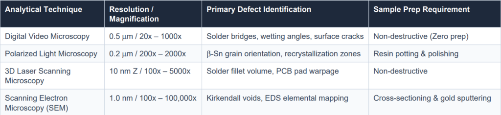
Final polishing utilizing 0.05 µm colloidal silica reveals the delicate Sn-grain orientation and Ag3Sn intermetallic platelet distribution. Polarized light microscopy exploits the optical anisotropy of body-centered tetragonal β-Sn grains, instantly revealing grain boundary misorientations and recrystallization zones induced by thermal cycling stress.
4. Industrial SMT Factory Deployment & Inline Reflow Verification
Deploying high-resolution digital inspection systems directly adjacent to SMT surface-mount reflow lines enables real-time process monitoring. By sampling 5 circuit boards per production lot immediately post-reflow, QA technicians inspect solde wetting angles (θ < 30° required), heel fillet height, and tombstoned micro-passives before conformal coating application.

5. Failure Analysis Methodology & Equipment Matrix
6. International Standards & IPC Compliance
Microscopic solder joint evaluation must strictly align with IPC-A-610 (‘Acceptability of Electronic Assemblies’) Class 3 standards for high-reliability aerospace and life-support electronics:
IPC-A-610 Class 3 Solder Requirements:
• Primary Side Fillet Height: Minimum 75% solder fill inside plated through-holes (PTH).
• Solder Wetting Angle: Contact angle θ must not exceed 30° for optimal metallic bonding.
• BGA Void Area Limit: Total X-ray/optical projected void area must not exceed 15% of the total ball area.
• Interfacial Micro-Cracking: Zero allowable crack propagation along the load-bearing pad interface.
7. Diagnostic Remediation & Process Optimization
A. Excessive IMC Layer Thickness (>4.0 µm): Caused by extended time-above-liquidus (TAL > 90 seconds) during reflow.
Remediation: Adjust reflow conveyor speed to restrict TAL between 45 and 60 seconds.
B. Kirkendall Void Formation: Caused by excessive thermal storage (>125°C for 500 hours).
Remediation: Apply nickel-barrier surface finishes (ENIG / ENEPIG) to suppress Cu-Sn solid-state interdiffusion.