Quality control is critical in electronics manufacturing. Even the smallest defect in a solder joint, circuit board, or microchip can lead to failures, costly rework, or safety risks. Traditional methods such as visual inspection and functional testing remain useful, but they cannot keep up with today’s miniaturized, complex, and multilayered electronic components.
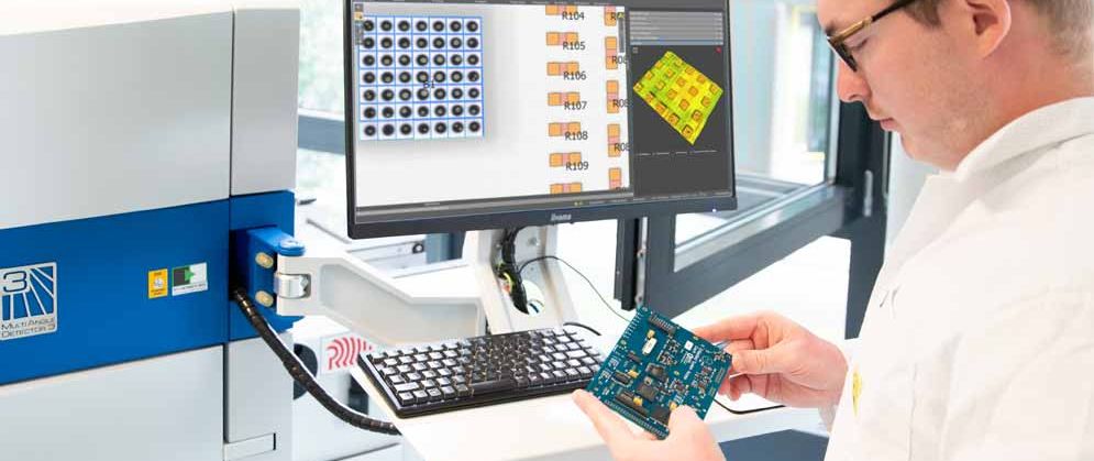
To address these challenges, manufacturers rely on X-Ray Inspection Systems. These systems provide non-destructive insight into hidden structures, enabling fast and accurate detection of defects that would otherwise remain invisible.
This article explores how X-Ray inspection works, its key advantages, and why it has become an essential tool in the electronics industry.
1. Why X-Ray Inspection is Important in Electronics Manufacturing
X-ray inspection systems, also called radiography systems, use X-rays to generate detailed images of an object’s internal structure. In electronics manufacturing, they allow manufacturers to check components and assemblies without causing damage. This makes them a reliable non-destructive testing (NDT) method that ensures quality and performance.
Key Functions of X-Ray Inspection:
Detects hidden defects inside components
Provides non-destructive internal imaging
Supports quality control and reliability checks
2. Visual Inspection vs X-Ray Inspection
Feature / Factor | Traditional Visual Inspection | X-Ray Inspection System |
Inspection Method | Surface-level only | Penetrates materials to reveal hidden defects |
Defect Detection | External flaws only | Internal voids, cracks, misalignments |
Accuracy | Operator-dependent | High-resolution, repeatable imaging |
Throughput | Manual, slower | Fast, automated (inline systems) |
Best Suited For | Simple, visible components | Complex PCBs, semiconductors, multilayer assemblies |
3. Types of X-Ray Inspection and How They Work
Types of X-Ray Inspection
2D X-Ray Inspection
- Produces flat, two-dimensional images of components.
- Suitable for quick checks and high-throughput production.
2.5D Oblique Angle Inspection
- Captures angled views to inspect hidden solder joints and overlapping structures.
- Commonly used in BGA (Ball Grid Array) inspection.
3D Computed Tomography (CT) X-Ray
- Creates detailed three-dimensional images of internal structures.
- Best suited for R&D, failure analysis, and critical BGA inspections.
How X-Ray Inspection Works
X-ray inspection is straightforward: an X-ray source emits radiation through a component, denser areas absorb more energy, and a detector captures the image. Software then analyzes it to reveal defects or misalignments. This process allows engineers to inspect internal structures without damaging the part.
4.Key Applications in Electronics Manufacturing
X-ray inspection is widely applied in:
- Solder Joint Analysis – Detects voids, cracks, and bridging in solder connections.
BGA and CSP Inspection – Ensures proper ball alignment, shape, and internal connections.
PCB Assembly Verification – Verifies correct component placement and identifies hidden defects.
Semiconductor Packaging – Examines wire bonding, die attach, and encapsulation quality.
Failure Analysis – Identifies root causes of defects without damaging the sample.
5.Technological Advancements and Benefits
Advancements in X-Ray Inspection Technology
X-ray inspection technology has evolved significantly, making it faster, more accurate, and easier to integrate into modern production lines. Some key advancements include:
- Higher Resolution Imaging – Detects even the smallest solder defects and micro-cracks.
3D Computed Tomography (CT) – Provides full 3D visualization for detailed failure analysis.
Automated Defect Detection – AI-powered systems reduce reliance on manual inspection and improve consistency.
Industry 4.0 Integration – Seamless connection with MES/ERP systems for real-time quality data.
Benefits of X-Ray Inspection Systems
- Enhanced Product Quality: Detects and addresses defects early in production, ensuring final products meet strict reliability standards and reducing recalls or failures.
- Increased Efficiency: Automated inspection systems process large volumes of components quickly and accurately, minimizing manual work and speeding up production.
- Cost Savings: Early defect detection prevents costly rework and scrap; improved yield and reduced waste lower overall production costs.
- Compliance and Certification: Helps manufacturers meet strict industry standards, essential for sectors like automotive, aerospace, and medical devices.
- Competitive Advantage: Advanced inspection technology enables higher-quality products, more efficient manufacturing, and a stronger market position.
6. Conclusion
X-ray inspection systems are now indispensable in electronics manufacturing. They allow manufacturers to detect hidden defects, ensure consistent product quality, optimize production efficiency, and reduce costs while maintaining compliance with industry standards. As these systems continue to advance, they provide the reliability and precision needed for increasingly miniaturized and complex electronic components. Investing in X-ray inspection technology is no longer optional; it is a critical factor for manufacturers striving to stay competitive and deliver high-quality products in today’s demanding market.