
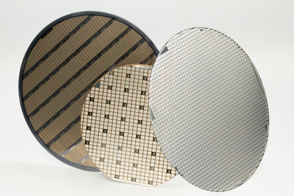
The electronics and semiconductor industry is built on precision. As chips and devices continue to shrink into the nanometer range, manufacturers need tools that can see, measure, and analyze features too small for the human eye. Scanning Electron Microscopy (SEM) is one of the most powerful solutions for this challenge.
SEM provides ultra-high-resolution imaging, nanoscale measurements, and detailed material analysis. It is used at every stage of semiconductor manufacturing—from research and development to production and quality assurance. Below, we explore the top applications of SEM in electronics and semiconductor production.
1. SEM for Failure Analysis
In high-tech manufacturing, even the smallest defect can lead to major losses. That’s why SEM is often the first tool engineers turn to when something goes wrong. Its ability to zoom into microscopic levels helps uncover problems that traditional inspections simply miss.
In semiconductors, SEM reveals wafer cracks, dislocations, and contamination that can quietly reduce yield if left unchecked.
In electronics, it helps spot hidden solder joint cracks, oxidation, or thin-film peeling that might cause early product failures.
By making these issues visible, SEM not only supports failure analysis but also provides insights for process improvement. This ensures higher reliability and fewer costly recalls down the line.
2. Materials Characterization
Every high-performance chip or circuit board depends on the right materials. SEM goes beyond surface imaging to analyze structure and composition with unmatched clarity.
For semiconductors, this means checking wafer surfaces, doping uniformity, and the fine structures inside transistors that affect speed and efficiency.
For electronics, it involves studying conductive coatings, insulating films, solder alloys, and bonding layers on PCBs.
This detailed material validation ensures consistency in electrical, thermal, and mechanical properties, reducing the risk of long-term failures.
3. Process Monitoring and Quality Control
Production lines need more than just speed they need precision at every step. SEM plays a critical role in verifying that processes stay within the tight tolerances required.
In semiconductors, SEM monitors etching depth, thin-film thickness, and lithography alignment during wafer fabrication.
In electronics, it checks solder paste deposition, microvia drilling, and component placement accuracy in PCB assembly.
By feeding this data back to production teams, SEM helps improve yield, reduce variation, and ensure consistency across high-volume manufacturing.
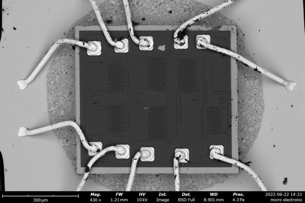
4. Packaging and Assembly Inspection
Even after chips are fabricated and boards are built, packaging and assembly remain critical for performance and reliability. SEM is widely used to verify that these final steps meet industry standards.
In semiconductors, engineers rely on SEM to inspect wire bonds, flip-chip connections, and protective encapsulation.
In electronics, it ensures solder joints are solid, connectors are properly aligned, and micro-assemblies meet design requirements.
This level of inspection prevents hidden weaknesses from slipping into final products, giving end-users greater confidence in device reliability.
5. Checking Circuit Patterns with SEM
As devices get smaller, the patterns used to build chips and electronic circuits must be extremely precise. Even the slightest error can affect performance or cause defects. SEM is the tool engineers use to make sure these patterns are accurate.
In semiconductors, SEM checks resist patterns, feature sizes, and alignment during the printing of microchip layers.
In electronics, it verifies fine PCB interconnects, dense wiring, and other advanced circuit features.
By confirming that every line and feature is printed correctly, SEM supports miniaturization while maintaining performance and reliability. This makes it a key tool as both industries push for smaller, faster, and more powerful devices.
6. SEM in Research and Development
Innovation doesn’t happen without experimentation. SEM gives R&D teams the tools they need to explore new materials and designs at the nanoscale.
For semiconductors, this includes testing wide-bandgap materials like GaN and SiC, developing 3D packaging methods, and analyzing prototype chips.
For electronics, SEM supports the design of next-generation PCBs, connectors, and sensors, while also evaluating new solder materials and joining techniques.
By offering deep insight during the development stage, SEM shortens the path from concept to market-ready product.
Conclusion: Why SEM Matters in Electronics and Semiconductor Production
The demand for advanced technology is pushing semiconductors and electronics to their limits, making Scanning Electron Microscopy (SEM) indispensable.
In semiconductor production, SEM delivers nanoscale imaging, defect detection, and precise metrology to ensure wafers, transistors, and advanced packaging meet the strict standards of today’s processors and memory devices. In electronics, it enhances reliability by analyzing solder joints, identifying PCB defects, and verifying packaging integrity in applications ranging from consumer devices to automotive and medical systems.
By enabling higher yield, lower costs, and consistent quality, SEM has become a cornerstone technology for both industries. As devices continue to shrink, increase in complexity, and demand greater performance, SEM will remain essential in driving innovation and ensuring long-term reliability.